
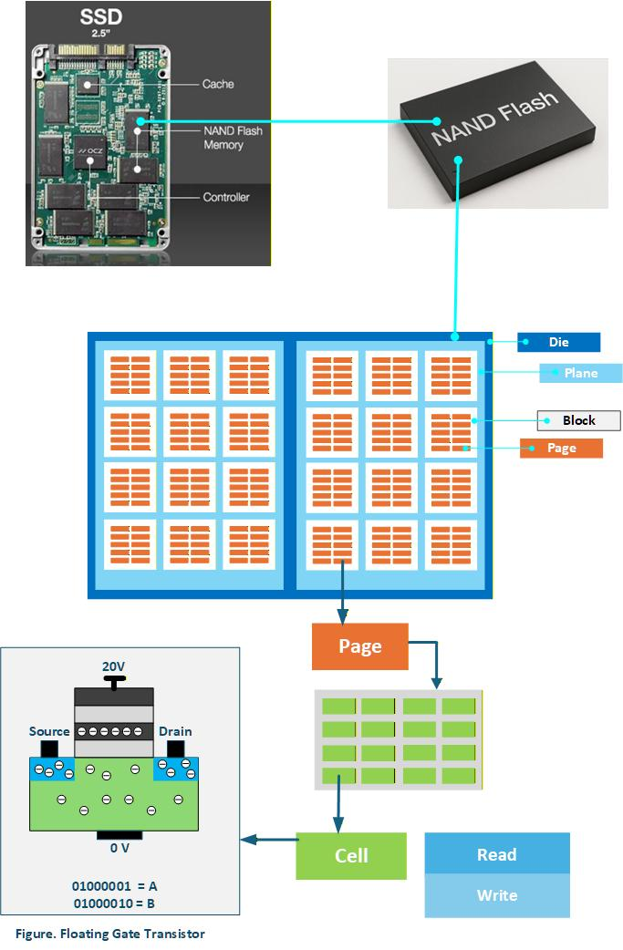
Figure 1:- Solid-State Drive (SSD) System Architecture Diagram
What is Solid-State Drive
As we know SSD most commonly used storage on Desktops and laptops. It uses flash memory similar to USB drives to store data instead of spinning disks like traditional Hard Disk Drives (HDDs)
In this blog, we discuss NAND flash memory, which is a non-volatile memory that is widely used in SSDs, USB drives, memory cards, and smartphones.
History Of SSD
In 2006, SSDs (solid-state drives) first entered the commercial market, marking a major turning point in storage history. Before 2006, SSD were mainly used in Military systems, Industrial machines, Supercomputers.
Figure 2. Floating Gate Transistor
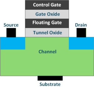
Die
└── Block
└── Page
└── Cell
└── Floating-Gate Transistor
Every memory cell = one floating-gate transistor.
How is data written, erased, and read in an SSD?
We will understand the basic operations involved in understanding how data is written, erased, and read in a NAND flash SSD.
1. Data Writing Operation – Basic Operation
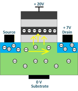
Control gate: High Voltage + 20V
Drain: High Voltage +7V
Source: Grounded (0 V)
Logic0
During the data writing process, a high voltage is applied to the control gate and drain. Electrons start to flow from source → channel → drain.
As this occurs, the control gate + positive charge attracts – negative charge in the channel. Some electrons gain sufficient energy to become hot electrons and penetrate the tunnel oxide, jumping into the floating gate.
The electrons get trapped inside the floating gate and cannot escape, even when the power is off.
This represents logical 0 → electrons trapped in the floating gate.
Logic 1 (erased state)
For logic 1, no voltage is applied to the transistor for programming. This is because the floating gate contains no trapped electrons, so no action is required — it is already in the logical 1 state.
Logic 1 are never “written” — they are simply left as-is. That’s why when we use a new SSD or a freshly formatted SSD, all memory cells are already in the logical 1 state (11111111). Writing data only changes bits from 1s → 0s.
Logic 1 → no electrons are trapped in the floating gate.
When we purchase a new SSD, it is formatted at the factory, so all bits are in the state of 1s.
New SSD → 11111111
Write SSD → 01110011 → ‘S’   > only 0s is written
As we can see, we are only writing 0s in a new SSD. That means we are turning on the transistor to write 0s, while not applying any voltage for 1s.
Note: There are two flash-memory writing methods. Don’t get confused.
1. Conventional Flash (CHEI)
Control Gate & Drain: High voltage
Source: Grounded
Example: SSD
2. SuperFlash (Source-Side Injection)
Control Gate & Source: High voltage
Drain: Grounded
Example: M.2 SSD
2. Data Erasure Operation – Basic Operation
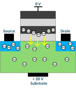
Data erasure is exactly the opposite of data writing, which involves grounding the Control Gate or applying a slightly negative voltage to the Control Gate, causing the negatively charged electrons in the Floating Gate to be attracted to the positive charge (substrate), penetrate through the tunnel oxide, and return to the Channel.
This makes logic 1 → no electrons on the Floating Gate.
Erase just removes most electrons from the floating gate, but:
- Some charge residue remains.
- The correct way to erase all bits to 1s is by using a flash erase (block erase) operation.
Note: When we delete any files on devices, they are logically deleted at the OS level, but physically some residue of electrons is still present in the floating gate.
That is the reason we can recover files even after deletion.
3. Data Reading Operation – Basic Operation
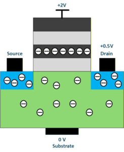
During reading, the stored value is determined by checking the amount of charge in the floating gate to see if it represents 0s or 1s.
Control gate: A small voltage is applied (+2 V – 4 V)
Drain: Low voltage (+0.5 V – 1 V)
Source: Grounded (0 V)
When voltage is applied to the control gate and drain, this is called the read voltage. If the read voltage is higher than the threshold voltage, the transistor turns ON, which means logic 1 — that means there are no electrons in the floating gate.
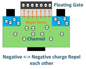
To read logic 0, when we apply read voltage, the read voltage is lower than the threshold voltage. This is because there are already electrons in the floating gate, which create a repulsive force between the negative charges in the floating gate and the channel. The read voltage is not enough to overcome this force, and the transistor doesn’t turn on. That is read as logic 0.
What is Threshold voltage ?
Threshold voltage is a property of the transistor. It is set during the data writing process.
When data is written as logic 0, electrons are trapped in the floating gate. The electrons (negative charge) in the floating gate and electrons (negative charge) in the channel repel each other, which makes it more difficult to turn ON the transistor.
Threshold voltage is the voltage required to overcome that repulsive effect. During data reading, a voltage higher than this threshold voltage must be applied to turn the transistor ON.